Do touch my packs, if you please, Mr. Customs man!

June 30, 2015

Must be some kind of planet
For all the people who can manage.
All of us who can handle it,
With all of this damage.

The Dandy Warhols, “Plan A”

It feels strange to type into WordPress after two years of complete abstinence and four years since any actual work on this project. It’s already year 2015, and last time I had something to say it was back in 2011! For sure, there is good reason for me writing a new post now. But let me not run too fast, or else I will spoil all the joy from readers. Instead of telling right away my reason for posting, I will start telling a story of how the things came, or what the goddess lady Fortuna (who may be the same person as the ancient Greek goddess Tyche) brought about.

Two and a half months ago, an email came in from a gentleman under the name of Victor, who lives in Canada. Victor stated he was interested in both my Open USB FXS and Open USB FXO projects. I patiently explained to him that Open USB FXO is very much in a complete failure state, and he should not expect anything working out of it. In vain. Victor insisted that he was sincerly and truly interested in the project whatever its status was, and he asked that I sent him any materials I had in order for him to build an Open USB FXO board.

Which I did: I unburied my forgotten carton box with the ingredients of Open USB FXO project out of inexistence, dag carefully into it and fished out what I had to in order to compile a kit. As a side note, never before had I compiled an Open USB FXO kit, because I would never pass to anyone something that doesn’t work. Compiling such a kit felt anyway strange…

Then, the package I sent to Victor probably was of great interest to the Canadian Customs Office, who withheld it for five (!) weeks of processing. I guess that, during this time, the Customs authorities had ample time to fully analyze the contents of the kit, make sure it did not contain any harmful substances, and even verify the correctness of the resistance values typed with miniscule letters on the tiny 603 resistors! They must have also had enough time to reverse-engineer the code flashed into the PIC 18LF2550 that was included with the kit into high-level C code, and I am pretty much sure that they checked on the BOM, too, and verified that the kit was complete. Anyways, it is good to know that there are interested hobbyists everywhere out there.

Against all odds, the fact that the Customs guys took their time to process my package was a lucky coincidence.

Why, might you ask. The answer is that, because in the meantime, Victor and I had the time to discuss a bit about the status of the project. And Victor, who proved a very methodical guy, not having in his hands an actual kit to play with, found it useful to devour (information-wise, that is…) the whole PIC18(L)F2x550 manual. And, when he came down to page numbered 362, he noticed that nice graph on Figure 28-2. What this graph says is that the maximum frequency of the PIC18LF2x550 is dependent on the supply voltage. Put in other words, the graph clearly said that this otherwise fine device will not run in 48MHz unless powered with 4.2V or more! No wonder my FXO board did not even start on USB power.

Victor just had found the (first, and doubtedly the only) flaw in my design. Open USB FXO, as currently designed, will never work. While at first it would seem that using a lower frequency is a workaround, actually it is not: the TMR1 interrupt service function that implements the PCM bus (you will have to consult my Open USB FXS blog for more information on what this function is and how it works) will not tick correctly unless the processor core is clocked at 48MHz.

So, what is next? How could we fix that? Well, there are two paths. Let me go back to the reasons for selecting a PIC 18LF2550 for this design: it all has to do with interfacing with the (3.3V) chip Si3050. Hence the trick with the BAV99 double diode, to drop the USB-supplied voltage to approx 3.3V. But then, this PIC will not work at 3.3V/48MHz. It must be powered at 5V. So, what could be done?

Solution #1 (and the one adopted by Victor) would be to stick to PIC18F2550@5V and use a 5V/3.3.V lever converter chip between the PIC and the Si3050. This would have to interface all the SPI and the PCM bus signals, namely SCLK, SDI, SDO, CE for SPI and FSYNC, PCLK, DRX and DTX for PCM. Plus the INT and RESET signals, this totals to 10 signals. Wow, that’s a lot!

Soluion #2 may be a bit more dangerous, and it’s the poor man’s equivalent. It consists in using the 18LF2550, still at 5V, and use resistor-based level reduction for the signals from the PIC to the Si3050 (SCLK, SDO, CE, FSYNC, PCLK, DTX). How about the other four? Well one could gamble on these, and attempt to interface them directly to the PIC18LF2550’s inputs. According to the manual, when powered at 5V, any input with a level of 2V or more is interpreted as a logical one. Logical one outputs from the Si3050 would be close to 3V, so that path looks safe enough (and cheaper than a level converter chip).

Again, I think that we owe much of this to the Canadian Customs authorities who have delayed the package. That’s why I used this, slightly rephrased lyrics from Arlo Guthry’s song “Coming into Los Angeles”. I guess Arlo was afraid of what the officers would find in his bags. While we were lucky they did check my package. I don’t know what they found. I know that all of us did: Victor found a solution, and the Open USB FXO project found a new father. It also found new hope of becoming a reality. A great thanks to Victor, goddess Tyche and the Customs! All of those who did handle it with all of this damage!

Google Code project created

February 7, 2013

Long time no hear! This was because I had nothing new to report. I did nothing new with Open USB FXO and I did not have the slightest idea why my prototype failed to work.

I still do not have the slightest idea. However, in a private conversation with one of the blog readers, I was convinced that letting people take a look at my work could help in spotting the error in my design, whatever this error is (this statement makes the funny assumption that the number of errors my design accounts to just one).

Therefore, I created a google code project for Open USB FXO. It can be found at http://openusbfxo.googlecode.com/, and the sources can be browsed at https://code.google.com/p/openusbfxo/source/browse.

Please do not take the correctness of any of the uploaded files (schematics, boards and libraries) for granted. They are uploaded just for public scrutiny and review, in the hope that someone else can spot this error that I cannot see myself. Hopefully someone will.

(Still) no satisfaction

September 13, 2011

It makes no sense to repeat the lyrics from Rolling Stones’ Satisfaction here. It’s a great song alright, but for some reason all that’s been left from it in my own mind is that recurring motto “I can’t get no”, which Mick Jagger shouts out angrily, over and over. That’s about my feeling, too, when trying to get my first Open USB FXO prototype to work: no satisfaction…

To take over from where I left in my previous post, it seems that the BAV 99 between the ICSP pinheader connector and the PIC is indeed a barrier to programming the 18LF2550 in-circuit using FDART2003 and WinPIC800. I have conducted a couple of web searches, trying to grasp how these two, the 18LF2550 and the FDART2003, get along with WinPIC800 as a programmer. The search showed that, although WinPIC does not reference the 18LF2550 as a supported chip, various people around have programmed successfully 18LF2550 PICs using the FDART2003 and WinPIC combination.

The only possibility that this left me with was that my circuitry with the BAV99 prohibited ICSP-programming the PIC on-board, at least with this programmer. This, in turn, meant that if I wanted to test my prototype design, I had to either change the culprit circuitry (e.g. providing a jumper that would bypass the BAV99), or to replace the PIC with another, pre-programmed one. Of course, if I chose the second path, I ‘d have to somehow pre-program another 18LF2550 — I am not good at unsoldering ICs without destroying them.

But wait — sure I could program another PIC. The First Principle for Prototype Designers states “One equals none”, and I had taken that very seriously: I had ordered materials for three prototypes, so there, sitting nicely in the pouches from Mouser, were another two 18LF2550. And I still had a host of un-populated Open USB FXS boards, which I could use as ICSP programming boards. All I had to do was to solder the RPGM resistor and short-circuit jumper J1. Then I ‘d have to place the PIC and hold it firmly on-board, and I ‘d be able to program it!

Naaaahh, might you think, that sort of thing will never work. Let me tell you: it had indeed worked in the past, because that’s exactly how I programmed all Open USB FXS PICs before soldering them for my first prototype bunch. So I was confident that I had a chance going down this path.

My first attempt though gave — no satisfaction. The WINPIC refused stubbornly to auto-detect the 18LF2550. But then, I decided to be more insistent than the damn PIC. I tried again, this time holding firmly with my hand one of my old PIC18F2550’s; it worked at once, revealing to WinPIC800 its internals. Well that couldn’t be… I tried again with the 18LF2550 and, bingo! It was recognized (as a 18F2550)! For some reason, the 18LF2550 needed more pressure force to make good contact on the PCB.

I programmed both my two remaining 18LF1550’s. Then I started with removing the unprogrammed LF2550 from the board by cutting the pins and removing the remnants with a soldering iron. I tried my best to cut the pins as gently as I could, but I still ruined a couple of pads. No problem; after soldering the new PIC in place, I soldered a couple of small wires right from the pins whose pads I had destroyed to the corresponding signals.

Then I tested the circuit. Which, you guessed it right, gave — no satisfaction… The PIC refuses to start. A few quick measurements show that the voltage at the cathode of the BAV99 is 3.9V which is OK (note that, when the circuit starts to work, it will draw some current and I expect the voltage to drop a bit, down to 3.5V or so). Well?

All that crosses my mind is “I can’t get no [the damn thing to work], ooh, no, no no…, no satisfaction… no satisfaction…”.

Admittedly, it’s too early. I need to conduct a thorough electrical test, and then I will again review my schematic to see if there is some glitch there. However, I thought this time things would be easier. Reality shows they are not. Stay tuned, there should be some news sooner or later!

The first Open USB FXO board (ever)

August 29, 2011

After a rather long design and culmination period, time finally has come for Open USB FXO to transmigrate and materialize from a series of blog posts into a real circuit — working or not. Most likely not: getting the thing working from the first shot seemed to me very, very ambitious.

These days, and after all my former Open USB FXS adventures, building a prototype had become sort of easy to me. I went through my BOM on Mouser and tried not to deviate too much from theoretical values. Some peculiar-valued resistors at 0.5W with a 1210 package were not stocked, so I had to trade-off for 0.4W instead, hoping that the final circuit will not blow smoke on me (a few calculations showed that this should not happen, but does one ever know?).

Going through the actual list shipped by Mouser, I felt a first shiver by running into two bags labeled “R1”. Mouser let you specify a “customer label” for every ordered component, on which the wise-thing-to-do is to put the “R1”, “R2”, etc. component names from your BOM. Unfortunately though, their otherwise good “BOM upload” tool that batch-uploads your BOM does not accept customer labels, so one has to enter them by hand. So there was my first bug: I had entered “R1” instead of “R11”. But the BOM was otherwise correct, so it sufficed to fix the “customer label” on one of the bags.

I submitted my Gerber files to Eurocircuits, who once more ignored the bottom-layer silk mask file that I produced, and turned in a perfect, two-sided-copper, single-sided-silk PCB. Actually, four of them, although their policy states that for ordering two pieces, one usually gets a third one for free. One bonus PCB was a great gift, thanks Eurocircuits!

It took me two afternoons of a working day to assemble my first prototype. So here are two shots of the first Open USB FXO board ever, right after assembly — and before cleaning, so the big ugly spots of dried soldering paste are clearly visible. The top side is here:

, and the bottom side is here:

Yes, I cleaned the boards after taking the pictures. Please share a minute with while we take a look at the PCB design and the component placement. After Silabs’ advice, the board is divided in two parts: the “line side”, facing the RJ11 connector and the “computer side”, facing the USB plug. The line side does not contain a ground plane; the only copper area is a little square one under the Si3019 that serves as a thermal for that chip. Other than that, the component placement resembles that of the FXS board: the PIC is on the bottom side, this time along with the MPU (Si3050); the line-driver chip (Si3019) is on the component side. Several tiny caps and resistors; the crystal; the programming switch; the “sidactor” line-protection device under the RJ11; the LED; that’s pretty much it.

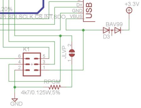
And of course, I realized my first pernicious design bug — the moment right after I finished assembling the board. What’s that? I think that it will be impossible to program that PIC over ICSP. Why? Take a look at the following detail from the schematic:

The supply voltage from the K1 (ICSP) connector is fed into the BAV99 diode, just like the VBUS voltage from USB. So far so good, since my ICSP has been designed for a Centronics-driven FD-ART2003 programmer, which will feed 5V into it. Passing pin 1 through BAV99 reduces the voltage fed to the PIC for programming it down to 3.3V or so. Good, since this voltage goes also to the Si3050, which does not like 5V. The PIC is 5V-tolerant, so PGC/PGD/PGM coming from Centronics at 5V will not harm it. All this is perfectly correct; what is, then, the problem? Well, the PGD signal (program data) is bidirectional. When the programmer tries to read it, this will come out as a 3.3V-logic-1 signal. Centronics, on the other hand, will expect a 5V signal. Zap… My so-far PIC programmer is very unlikely to work under these conditions.

All this, let aside the fact that the PICLF2550 is not in the list of supported PICs of the WinPIC800 PIC programmer.

Yeah, but probably the author of WinPIC forgot the LF2550 out of the list? Probably Centronics will read 3.3V as a logical true? Well, why not give all this a try, you migth think. Let me save you some time; it’s not like I didn’t try. Of course it did not work.

So, after all that, I am now in a funny position where I am gazing at my first ready-made prototype board, which however I am totally unable to bootstrap it by programming the PIC bootloader firmware into it. What a bummer!

I have still one more thing to try: I can use one of my un-assembled FXS boards with the minimum required components (RPGM, KICSP and JLVP), and secure the 18LF2550 onto it with a clothes peg. Then I can try programming the PIC under a straight 5V environment. And, finally, I will take the pre-programmed PIC and mount it on my FXO prototype. OK, this is a path I will try; and if it doesn’t work, I ‘ll try to find me a real PIC programmer that can do the 18LF2550.

Whatever path I choose, news should be coming, sooner or later. I should be able to program the PIC, one way or another. So bear with me, dear readers. The long debugging trip of Open USB FXO has just begun!

A fast-growing baby

August 9, 2011

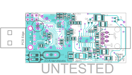
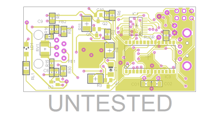
Since I found out about the low-power PIC18LF2550, development of my FXO project took off. I sat quite a few hours to correct my schematic and then fix a PCB that I had already semi-prepared. Here, then, is the latest schematic:

You can click on the above image to get a more readable view. You cannot miss the big “UNTESTED” seal on the schematic. This is just to give a warning that the circuit has not yet been tested and thus I do not advise anyone to try it out. And here are the top and the bottom PCB views, both with the same warning:

So, my next steps were to export my BOM and to order the materials (I used Mouser, since I could not find any other store selling Silabs chips on retail). In the next few days I will also place an order for the prototype PCBs and when I get back home from holidays (yes, I am typing this post while on holidays), I will start with assembling my first three prototypes.

So, isn’t Open USB FXO a really fast-growing baby? I just hope it’s not too fast, that is, that I have not made any big mistakes in my haste. But what is prototyping for, if not for finding out exactly this? Reality will show anyway. So, I am leaving this post as it is now and getting back into exporting my Eagle files in Gerber format and ordering my PCBs. Updates may follow later on. Good luck!

Did you connect the power plug?

July 15, 2011

The title of this post refers to the standard question from technical support, when one reports a problem with an electrical or electronic appliance over the phone: “is the power cable of your XYZ plugged into the mains outlet”? In this case, XYZ parallels to my brains, and the mains outlet  is something like the outlet of the universal common sense supply (let us assume that this supply exists anyway — and that it has an outlet somewhere…). This post explains why.

I had not written any new post on Open USB FXO since April. In reality, I was barely even thinking about my new project. The official excuse was that my new daytime job occupied just about all of my time. However, I believe that there was a slightly more complex (and much more sensere) explanation: because of the transition from the 18F2550 to the 18F25J50, this new project was now looking too complicated to me. I had already gone once through the realy early stages of design and development, back when I played with that first PIC development board (the one that refused to work unless I held it tenderly in my hands? Remember that?); I had invested much time into learning the PIC compiler and Microchip’s USB libraries; had made my first unsuccessful attempts in creating PIC firmware; and generally, I had stumbled upon every possible obstacle there was during these first steps. If I were to start over with a new processor, I would have to go through the same again — at least, so I was fearing. And I guess that this was what was really scaring me off my newborn FXO project.

Nevertheless, I started some work on the project: I first set to change the (open-source) Eagle library that I was using for the PIC 18F2550 into one for the 18F25J50. The 18F25J50 has vastly different pin names, and producing a schematic with the wrong pin names might work in practice, but would look ugly. The original library already conained the symbol and package formats that I needed, so what was remaining would just be a work of changing pin names. So, starting from the “microchip-pic18fxx5x.lbr” library that I used originally, I removed unneeded packages and symbols and changed the pins of the 18F2550 into the ones of the 18F25J50.

Now, funny, see how working in an open source context changed my view of the project.

Working in open source means sharing your work. If I were to give this new PIC18FXXJYY Eagle library away to others, I had to make it correct.  Changing the pin names would not suffice: as a final touch, I had to correct the HTML markup for the documentation of the library. It was then that I noticed that the original library also mentioned the PIC18LFxx5x, stating that this L stood for “low-voltage” — low whaaaaat?

A quick look into PIC18F2550’s datasheet confirmed that there is a low-voltage cousin of the 18F2550 that I used, namely 18LF2550. No wonder I had not noticed that so far; here is the only reference to “LF” that exists in the datasheet:

Standard devices with Enhanced Flash memory, designated with an “F” in the part number (such as PIC18F2550), accommodate an operating VDD range of 4.2V to 5.5V. Low-voltage parts, designated by “LF” (such as PIC18LF2550), function over an extended VDD range of 2.0V to 5.5V. 

No wonder I had missed that among the hundreds of pages of the datasheet (yes, I know this is no excuse)… Which means that there was a PIC18LF2550, that suited perfectly my needs, without needing to change anything substantial in my design. A quick lookup on Mouser revealed that not only did LF2550 exist, but also that it was in stock and priced quite the same as the F2550. In other words, all these redesign issues that gave me headaches could just vanish by using the 18LF2550!

A small change in the circuit would be required anyway for lowering the voltage to 3.3V. In the point where the circuit draws power from USB:

, I would have to add the two 1N4148 diodes that I mentioned in my previous post, just like this:

, and that would be it. Elementary… And this means that I can use my compiler, my hand-made FD-ART2003 PIC programmer, my flash memory utilities and my firmware without changing anything but the logic that interfaces with the Silicon Labs chipset.

So, after I connected my brains to the universal common sense supply (there had to exist a low-voltage equivalent of the 18F2550, and I should have thought about it before looking at another PIC), the project seems much easier to me, and I can start spending late-night or early-morning hours on it again. The little brother  just grew up a bit, after being stuck in its newborn state for quite some time.

Quick update, Jul 18: I think I will replace the two 1N4148 diodes with a BAV99 double-diode, in order to save some room in the PCB. I am now checking whether other designs use BAV99 successfully for dropping 5V to 3.3V. Anyone who can contribute on this, comments welcome!

Giving birth is not an easy thing

April 5, 2011

See there!  A son is born — and we pronounce him fit to fight.
There are blackheads on his shoulders, and he pees himself in the night.
We’ll make a man of him put him to trade
teach him to play Monopoly and to sing in the rain.

The lyrics above are from Ian Anderson’s “Thick as a brick”. A bit sarcastic, I agree, but they somehow felt fit for what is going to follow in this blog. See there, a(nother) Open FXx circuit is born! After Open USB FXS has gotten itself into a relatively mature state, I thought, what the heck, why not give that poor FXS circuit a little brother to keep it company? And thus came Open USB FXO.

What is Open USB FXO — or, more correctly, what will it be when it grows up enough to see itself becoming a real circuit? The answer is “a Foreign eXchange Office” adapter, able to connect your computer to the PTT plug on the wall. Forgot to say, your computer will have to run Linux and Asterisk.

I decided to start with an Open USB FXO circuit design by the end of 2010. Other tasks kept me away from posting any details about it until March 2011. Soon I came up with the following schematic (warning! it’s not ready and it’s not going to work!):

Cannot make out anything on the picture above? Try clicking on it and you will get a zoomed-in version that’s readable (though if you cannot make out the big, red warning, you may need eyeglasses — I ‘ll come back to that warning in a second).

Wow, might you think, this schematic is already too advanced! How did that guy come up with it? Well, let me help you change your mind. Much like Open USB FXS, the schematic above is little more than a port of the manufacturer’s reference application circuit. Engineering starts from selecting the telephony chipset, in this case Silicon Labs’ Si3050, together with the line driver chip, Si3019. From then on, what I did as a designer was just to take a look at the manufacturer’s data sheet, import that into CadSoft Eagle and add the same PIC-based front-end that I already had from Open USB FXS — voilà, here came Open USB FXO!

And then it took less than ten minutes to figure out that this was all wrong.

How come? Well, I overlooked a slight detail: contrarily to the Si3210 in my Open USB FXS design, the Si3050 operates at 3.3V. The PIC 18F2550 operates at 5V. They do not interface, full stop. So much for my wonderful first-try design.

Thus, there were two things that I could do: use a 5V/3.3V level converter chip to interface between the 18F2550 and the 3050, or use a different microcontroller that operates at 3.3V. I quickly dropped the first alternative, because it would make the circuit too complicated and add to its cost. Starting with the second alternative, I had already invested much into learning the architecture, the instruction set, the USB idiosyncracies, and the inners of the PIC 18F2550 to let all that go. So, I looked for a different PIC that would be as much as possible compatible with the 18F2550 but operate at 3.3V. That did not take too long to spot: it was the 18F25J50.

At first, the two chips looked pin-compatible, and thus I thought that I could just replace the 18F25J50 in the schematic. Halas, I was once more wrong. There are quite a few differences between the two chips:

  1. The 18F25J50 has about one zillion new special-function registers that do not exist in the 15F2550 (but OK, if I did not need these, I did not have to learn about them all, did I?).
  2. The clock modes are different. However, the 18F25J50 datasheet lists a 20MHz/divide-by-5 option that is compatible with that of  the 18F2550 (needless to say: I ‘d have to stick with 48 MHz core clocking if I wanted to re-use my TMR1 data-handling routine from Open USB FXS).
  3. ICSP programming is different. The 18F25J50 does not have a VPP pin, and uses \MCLR instead (\ stands for “not”: the pin has inverted logic). But then, \MCLR cannot be connected directly to VDD as in my former design, and needs a typical 1k-10k pull-up.
  4. The actual core of the 18F25J50 runs at an even lower voltage, 2.5 V. Of course, the chip has an internal regulator that supplies this voltage. To use that regulator, an external pin (pin 6, called VDDCORE in 18F25J50, which has taken the place of 18F2550’s RA4, which, in turn, has vanished in 18F25J50) needs to be connected via a capacitor to VSS.
  5. The 18F25J50 does not have an EEPROM (puff! — there goes the nice code I developed for storing a board ID and the auto-bootloader…or maybe not? Michrochip have a promising Application Note on their site called “Emulating Data EEPROM for PIC18 and PIC24 Microcontrollers” on their site).
  6. I am not sure whether the bootloader software that I have been using for the 15F2550 will work on the 15F25J50. Maybe it will need modifications. But there is a nice Application Note on that as well.
  7. And then, of course, I would need to adjust VDD from the USB-supplied 5V to 3.3V. A couple of 1N4148 diodes in series would do that alright, yielding about 3.6-3.4 V depending on the actual diode make and the current drawn.
  8. (update, Apr 10): And it seems that the list doesn’t end here; the SDI and SCK pins are also in different places… I am checking for more diffs, while creating the Eagle library for the 25J50. (Update, Apr 12): However, the 25J50 has software-programmable I/O pins, among which are the SPI2 pins (SDI2, SDO2, SCK2). I might program these to coincide with the pins of the 2550’s SPI, and thus save me the additional changes in the schematic. Perfect!

So here is where I stand right now. I am studying the data sheet and the Application Notes to see if I can use the PIC18F25J50. I think in the end I ‘ll manage it, but who knows… Giving birth is not an easy thing, it seems. Especially if the parent is a guy like me, who first puts down a design and then consults the data sheets. Nevertheless, let us be optimistic. It’s a newborn circuit after all, so let us show it –and its parent– some forgiveness for all the small and big mistakes it contains in its design, and hope that they will get eventually all fixed. Hey, welcome to life, Open USB FXO!